Index Of The Blog
In today’s fast-paced electronics landscape, the downsizing of devices is receiving significant attention. As the demand for more compact and efficient electronics grows, printed circuit board (PCB) design has been revolutionized.
The miniaturization of PCBs has transformed the electronics industry by enabling the creation of smaller yet more powerful devices used in fields like medicine and aerospace. Aspiring engineers and designers interested in PCB design would benefit greatly from taking a PCB design course to gain the skills needed to keep up with this rapidly progressing field.
This article explores the importance of miniaturization in PCB design and its impact on electronics. It provides insights valuable for those pursuing a career in this area.
The shrinking of PCBs has been a game-changer, allowing for the development of tinier but more capable electronics in healthcare and space travel. Engineers and designers looking to understand PCB design better would benefit from focused coursework to build the expertise needed to match the speed of change in electronics.
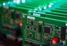

Table of Contents:
- What is miniaturization in PCB design?
- Importance of miniaturization in PCB design
- Advantages of miniaturization in PCB design
- Challenges in the miniaturization of PCBs
- Techniques for miniaturization of PCBs
- Applications of miniaturized PCBs
- Future of miniaturization in PCB design
- Conclusion
What is Miniaturization in PCB Design?
Miniaturization in PCB design refers to reducing the size of electronic components and the PCB itself while maintaining or improving its functionality. It involves using advanced manufacturing techniques, materials, and design processes to reduce the size of electronic devices and improve their performance.
Importance of Miniaturization in PCB Design
The importance of miniaturization in PCB design cannot be overstated. In today’s world, where portability and convenience are highly valued, miniaturization allows for the development of smaller, more efficient electronic devices. This is especially important for industries such as medical and aerospace, where space and weight limitations are critical factors. Miniaturization has also led to the integration of more features into a single device, such as GPS, Wi-Fi, and Bluetooth connectivity.
Moreover, miniaturization has also reduced production costs, making electronic devices more affordable and accessible to consumers. By reducing the number of components required and increasing the efficiency of the manufacturing process, miniaturization has made it possible to produce electronic devices at a lower cost.
Advantages of Miniaturization in PCB Design
The miniaturization of PCBs has fueled tremendous advances in the electronics industry. It has paved the way for highly portable, optimized, multi-functional, and cost-effective smart devices that enrich and simplify our lives in many ways. With continued progress in miniaturization, there are sure to be many exciting innovations on the horizon.
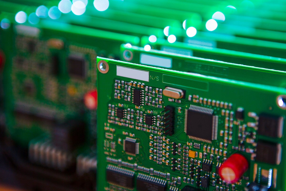
The miniaturization of printed circuit boards (PCBs) has led to significant advantages in electronic device design. By making components smaller and packing them into a tighter space, miniaturization allows for more portable, high-performance, and cost-effective electronics.
Increased Portability and Convenience
Miniaturization allows the creation of smaller and more portable devices like smartphones, laptops, and wearables. These compact designs provide users with more convenience and flexibility.
Improved Performance
Components are placed closer together on a PCB, performance is enhanced in several ways. Signals have less distance to travel, so there is less interference and distortion. Power usage also decreases due to shorter trace lengths. All of this allows for faster processing speeds and higher functionality.
Reduced Cost
Miniaturization lowers production costs using fewer, smaller components and more efficient manufacturing techniques. This makes high-tech devices more affordable and accessible to a wider range of customers.
Increased Functionality
Miniaturization provides more space for additional features like GPS, Wi-Fi, Bluetooth, and more. All of these capabilities can be integrated into a single, small device. This convergence of functions into one compact product adds significant value for users.
Challenges in the miniaturization of PCBs
While miniaturization offers several benefits, several challenges must be overcome. Some of the challenges in the miniaturization of PCBs include:
- Thermal Management: As components are packed closer, heat dissipation becomes more complex, leading to overheating and reduced performance.
- Signal Integrity: As the distance between components is reduced, signal integrity becomes more important and can be affected by noise, interference, and crosstalk.
- Manufacturing Complexity: As components become smaller, manufacturing processes become more complex and require more advanced techniques and equipment.
- Reliability: Miniaturization can also lead to reduced reliability due to the increased risk of component failure and difficulty in maintenance and repair.
Techniques for Miniaturization of PCBs
There are several techniques used in the miniaturization of PCBs, including:
- Surface Mount Technology (SMT): SMT involves mounting components directly onto the surface of the PCB, allowing for smaller and more densely packed components.
- High-Density Interconnect (HDI): HDI involves using advanced manufacturing techniques to create smaller, more complex PCBs, such as micro and blind vias.
- Multi-layer PCBs: Multi-layer PCBs allow more components to be packed into a smaller space using multiple conductive material layers.
- 3D printing: 3D printing allows for creating complex and customized components, reducing the size and weight of electronic devices.
Applications of Miniaturized PCBs
Miniaturized PCBs have a wide range of applications, including:
- Consumer Electronics: Miniaturization has revolutionized the consumer electronics industry, enabling the development of smartphones, tablets, and wearable technology. These electronic devices have become smaller, lighter, and more powerful, making them easier to carry and use on the go.
- Medical Devices: Miniaturized PCBs are used extensively in medical devices such as implantable devices, diagnostic equipment, and monitoring devices. They are critical in developing cutting-edge medical technology, including pacemakers, insulin pumps, and implantable defibrillators.
- Aerospace Technology: Miniaturized PCBs, such as satellites and unmanned aerial vehicles, are used extensively in aerospace technology. They are essential in developing lightweight and compact electronic systems that can withstand space and high altitude conditions.
- Automotive Industry: Miniaturized PCBs are used in the automotive industry, such as engine control units, infotainment systems, and advanced driver assistance systems. They play a critical role in the development of safer and more efficient vehicles.
- Industrial Automation: Miniaturized PCBs are used in industrial automation systems, such as robotics and control systems. They enable the development of more compact and efficient industrial systems, resulting in increased productivity and reduced costs.
- Defense and Security: Miniaturized PCBs are used in defense and security applications, such as surveillance systems, communication systems, and unmanned vehicles. They enable the development of lightweight and compact electronic systems that can operate reliably in harsh environments.
Future of Miniaturization in PCB Design
The future of miniaturization in PCB design looks promising, with the continued development of advanced manufacturing techniques and materials. The use of artificial intelligence and machine learning in PCB design and manufacturing is also expected to play a significant role in the future of miniaturization.
Conclusion
Miniaturization in PCB design is essential for developing smaller, more efficient, and more powerful electronic devices. While there are several challenges to overcome, the benefits of miniaturization are significant, including increased portability, improved performance, and reduced cost. With the continued development of advanced manufacturing techniques and materials, the future of miniaturization in PCB design looks promising.